| Intel has high hopes for its Deschutes-series Pentium II
processors, which made their debut on January 26. If
successful, Deschutes will be the turning point in Intel's
campaign to make the Pentium II a mass-market product,
phase out the Pentium, bring sixth-generation x86
technology to mobile systems, and render the Socket 7
interface obsolete. Deschutes could also strengthen Intel's influence over the PC standard and, later this year, offer more diverse options for both high- and low-end PCs. All things considered, it's a lot to expect from a single product that essentially introduces no new features. No new features? How can that be? If you're confused, join the club. No other Intel processor has been surrounded by as much market confusion as Deschutes. Contrary to widespread belief, Deschutes implies nothing about the chip's core clock frequency, front-side bus speed, back-side bus speed, cache size, CPU interface, MMX, or system chip set. Deschutes is merely Intel's code name for a Pentium II processor manufactured on a 0.25-micron CMOS process. Nothing else distinguishes the Deschutes-series Pentium II from today's Klamath-series Pentium II. However, the smaller, more efficient process technology does mean Deschutes will run faster and cooler while consuming less power. That's why the first Deschutes attains a core frequency of 333 MHz — 11 percent faster than Klamath's top speed of 300 MHz — with a die size of only 131 square millimeters, compared to 202 square millimeters for Klamath-series Pentium II chips. Power consumption is only 23.7 W at 333 MHz, compared to 43 W for a 300-MHz Klamath. In all other respects, the initial implementation of Deschutes is identical to Klamath. Both CPUs come packaged in a Single Edge Contact (SEC) cartridge that fits Intel's proprietary Slot 1 interface. Both CPUs have the same P6 microarchitecture, including MMX and 32 KB of L1 cache memory. Both have a 66-MHz front-side (CPU to system memory) bus. Both have an external 512-KB L2 cache made of industry-standard burst static RAMs (BSRAMs), which are contained in the SEC cartridge. Both processors drive the L2 cache at half the CPU core frequency. Both work with Intel's 440FX and 440LX chip sets, and others from third parties. Both the Klamath and the initial Deschutes are limited by Intel's current CPU interface and system chip sets to a maximum of a two-way multiprocessing implementation. Later versions of Deschutes that target the sub-$1000 PC market will be more diverse (see the table), and new system chip sets will let Deschutes go beyond two-way multiprocessing this year. In the second quarter, Intel plans to roll out Deschutes processors at 233 and 266 MHz for mobile systems, followed by a 300-MHz mobile chip in the third quarter. All will dissipate 8 W or less. This will mark the debut of sixth-generation x86 technology in mobile PCs, allowing Intel to begin phasing out the Pentium for both mobile and desktop systems. Late in the second quarter, Intel plans to ship Deschutes processors at 350 and 400 MHz. Those chips will still drive the back-side (L2 cache) bus at half the core frequency and will have 512 KB of L2 cache memory, but the front-side bus will cruise at 100 MHz. Accompanying them will be Intel's new 440BX system chip set, which supports the 100-MHz bus. In June or July, Intel plans to deliver higher-end Deschutes chips for PC workstations and servers. Those CPUs will also have core frequencies of 350 and 400 MHz, along with the 100-MHz front-side bus. But they will drive the back-side bus at the full core speed. That will require Intel to divert precious foundry capacity to making superspeed BSRAM chips, because nobody else makes chips that fast in the quantities Intel needs. L2 cache sizes for those high-end CPUs will be 512 KB, 1 MB, or 2 MB. To accommodate the larger caches, the CPUs will come in a larger SEC cartridge that fits Intel's new Slot 2 (for more information, see "Sorting Out the Slots," November 1997 BYTE, page 74). And Intel will introduce a high-end chip set, the 450NX, that supports glueless four-way multiprocessing, which should make it almost as easy to design a multiprocessor system as it is to design a uniprocessor one. In the second half of the year, clock speeds will rise to 450 MHz for both the Slot 1 and Slot 2 Deschutes. Both will support the 100-MHz system bus and new chip sets. Meanwhile, Intel is scrambling to respond to the sudden downward shift in PC prices, especially the hot sub-$1000 market. Around midyear, Intel plans to release a stripped-down Deschutes that doesn't have an L2 cache and comes in a cheaper cartridge. Later, Intel hopes to ship new versions of Deschutes that have L2 caches of 128 and 256 KB that are integrated on the same die as the CPU core. Thanks again to the smaller die size that the 0.25-micron process allows, it's more practical now for Intel to integrate the secondary cache. The on-chip L2 cache would run at the full core CPU frequency, delivering good performance at low prices. This parallels the plans of AMD and Centaur Technology, who are also working on CPUs with integrated L2 caches. Intel is likely to introduce a new chip set and a new type of motherboard to accompany the lower-priced processors. The chip set, known as the 440LXR, is rumored to be a low-end 440LX. It will probably allow fewer expansion slots (PCI, ISA, SIMM, and dual in-line memory module [DIMM]) and will have no support for multiprocessing. However, it may retain support for an Accelerated Graphics Port (AGP). The new motherboard, known as the Micro ATX, is smaller than a full-size ATX because it has fewer slots. All these measures will lower Intel's costs a few dollars, but they'll also negate one of the technical advantages Intel claims for its proprietary CPU interfaces. By omitting or integrating the L2 cache in low-cost versions of Deschutes, Intel is eliminating the need for an external back-side bus — one of Intel's justifications for switching to slots. Either low-cost Deschutes could work just as well in Socket 7. In fact, a Socket 7 processor with an L2 cache might outperform a cacheless Pentium II. Intel says it will still be easier to upgrade a CPU that fits a slot instead of a socket. But that depends on how Intel modifies the SEC cartridge to cut costs. If Intel discards the cartridge housing to reduce costs, the bare daughterboard would be as vulnerable to static electricity and other handling hazards as a conventional chip. The advantage of proprietary slots, for Intel, is that they prevent competitors from selling CPUs that fit the same motherboards as Intel's. The sooner Intel can establish the Pentium II as the mainstream standard, the faster it can phase out Pentium-class CPUs and Socket 7 motherboards. Deschutes is a key step in that direction.
*The 440FX and 440LX may also support the low-cost Deschutes. 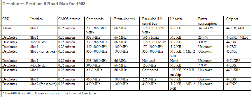  Copyright1994-1998 BYTE |