| [Editor's note: This
article was originally scheduled for publication in the
September 1998 issue of BYTE Magazine but was canceled when BYTE folded in
June 1998. It appeared instead in Windows NT Magazine
and in C'T, a
German computer magazine. This text is
the original English version.] While the world waits for Intel's 64-bit Merced chip and Microsoft's 64-bit version of Windows NT, Digital Equipment is offering a sneak preview of the next generation in NT processing. The Alpha 21264 is a 64-bit processor that runs NT. It's one of the fastest chips in the world. And it's available today. The 21264 is the latest generation of the Alpha microprocessor architecture. Digital expects the 21264 to reach clock speeds of more than 700MHz this year, so this processor upholds the speed demon reputation that the 21164 and 21064 established for Alpha chips. Alpha is the last RISC architecture for which Microsoft is developing future versions of NT. Microsoft is phasing out NT for MIPS Rx000 chips, and the PowerPC NT never really got off the ground. The only other CPU architecture that runs NT is, of course, Intel x86. Despite Intel's market dominance, the Alpha has one big advantage over the x86: increased performance, especially performance of floating-point tasks. Alpha systems generally cost more than their Intel counterparts, but Alpha systems are faster, and they excel at math-intensive engineering and scientific applications. To move beyond the performance limitations of the 20-year-old x86, Intel partnered with HP in 1994 to develop a new CPU architecture: Intel Architecture-64 (IA-64). Intel expects systems that use the Merced processor, the first processor to implement IA-64, to ship in mid-2000. But the Merced might not be the fastest chip on the NT market in 2000. Digital says that by the time Merced appears, the 21264 will be running at a clock frequency of 1000MHz (1 gigahertz [GHz]). At that speed, the 21264 will be substantially faster than the Merced according to estimated CPU benchmarks. (For a review of 21264 speeds, see Figure 1.) Digital said the first 21264 systems would hit the streets in late 1998, so you don't have to wait two years for 64-bit performance. However, the 21264 won't reach its potential until Microsoft ships a 64-bit version of NT for both IA-64 and Alpha chips. (Microsoft hopes to ship the 64-bit NT in 2000.) Whither RISC? The race between the 21264 and IA-64 processors is not just a subject of idle gossip. At stake is nothing less than the future of RISC for NT and every other operating system (OS). Outside of the highly specialized embedded-application market, RISC is in retreat. Currently, the most popular RISC architecture for the desktop is the PowerPC chip, which IBM and Motorola produce jointly. But the largest customer for desktop PowerPC chips is Apple, and the Macintosh has only about 4 percent of the PC market share according to International Data Corporation (IDC). In June, IBM and Motorola announced that they are dissolving their 7-year PowerPC partnership and will develop future PowerPC chips separately. IBM's other RISC architecture, the Power series, is merging with the PowerPC. IBM is phasing out the Power chip as a distinct architecture. The new 64-bit Power3 chip is the first processor that unifies Power and PowerPC technologies. Battling recent losses, Silicon Graphics is moving away from its MIPS Rx000-series RISC processors. Silicon Graphics canceled its next-generation Rx000 projects and recently spun off the embedded-chip portion of MIPS Technologies as a separate company. Silicon Graphics is developing x86-based systems for NT and porting IRIX to IA-64. Sun Microsystems is porting Solaris to IA-64. That move has prompted some industry analysts to speculate that the new UltraSPARC-III will be the last major generation of the SPARC family, although Sun claims that the rumors are false. HP is porting HP-UX to IA-64 as part of its strategy to move away from Precision Architecture-RISC. PA-RISC will gradually exit the market after IA-64 debuts. IA-64 will be backward compatible with PA-RISC. The Alpha is the fastest RISC chip according to most CPU benchmarks and the only NT alternative to the x86. But the Alpha's future isn't certain because of recent shakeups at Digital. The company sold its chip foundry in Hudson, Massachusetts, to Intel. Despite some misleading news reports, Digital sold only the foundry, not the Alpha. Digital will continue to independently design Alpha processors but will farm out the chips' manufacturing to Intel and other licensees. The two current Alpha-manufacturing licensees are Samsung and Mitsubishi. Digital is also negotiating deals with AMD and IBM Microelectronics. Mitsubishi currently has no plans to manufacture the 21264, although the company continues to provide technical support for the low-cost 21164PC chips it manufactured. Samsung has emerged as the most aggressive Alpha licensee. It recently formed a subsidiary to market Alpha chips and says it will push the 21264 to 1GHz by 2000. Compaq's acquisition of Digital makes the Alpha's fate more uncertain. Compaq has never owned a CPU architecture, and the company is one of Intel's largest customers for x86 chips. David Jessel, the Alpha's senior product manager, claims that Alpha fans have nothing to worry about. "Compaq has been fully supportive of the Alpha and is continuing to invest in it," Jessel said. To underscore its commitment to the Alpha, Compaq plans to substitute the 21264 for MIPS processors in its high-end Tandem servers. If the Alpha survives all these transitions, it could seriously challenge IA-64 chips for performance supremacy in the next decade. A technical analysis of the 21264 shows that the Alpha has plenty of room to become more powerful. Inside the 21264 The 21264 has an innovative design that departs significantly from the 21164's design. The new chip has larger primary caches, additional functional units, more accurate branch prediction, new motion video instructions (MVI), and high bus bandwidth. It executes as many as six instructions per clock cycle and sustains four instructions per clock cycle. In addition, the 21264 is the first Alpha to offer out-of-order execution. Out-of-order execution is a feature common to many microprocessors. Now that the Alpha offers this feature, Sun's SPARC chips are the only leading CPUs that don't execute instructions out of order. CPUs that run out of order dynamically rearrange a program's instructions at runtime to use the chip's resources efficiently. For example, if an instruction needs an integer unit but all the CPU's integer units are busy, an out-of-order CPU dispatches floating-point instructions to available floating-point units (FPUs) while holding the stalled integer instruction until an integer unit becomes available. When an integer unit becomes available, the CPU releases the stalled instruction. In the same situation, conventional in-order CPUs stall all instructions until the integer unit is free. Out-of-order CPUs always retire results in their original program order. Out-of-order execution used to be a characteristic of only brainiac processors, CPUs that rely on sophisticated instruction handling, not high clock speeds, to achieve top performance. The complex logic that manages older chips' out-of-order technique rules out high clock speeds. Previous Alpha chips ran at industry-leading speeds because they did not process instructions out of order. The 21264 breaks from that tradition. Available at 500MHz and 600MHz, it's definitely fast. And it will become faster. Digital says the 21264 will hit 733MHz this year and 1GHz within 2 years. But the 21264 is also a brainiac. It executes instructions out of order, and it does so more deftly than any other processor. The best way to evaluate the 21264's out-of-order efficiency is to examine the number of instructions it arranges at once. The more instructions an out-of-order CPU holds at one time, the more efficient its processing is because juggling many instructions gives a CPU a broader view of a running program's needs. However, this juggling act requires resources that in-order processing doesn't require: reorder logic, temporary registers to hold values for pending instructions, interlock circuitry to check for dependencies, and logic to retire the results in program order. Intel's P6 chips (Pentium Pros, Pentium IIs, Celerons, and Pentium II Xeons) juggle as many as 40 instructions simultaneously. HP's PA-8000 handles 56 instructions at once. The 21264 juggles 80 instructions, more instructions than any other processor. Digital implemented a clever register scheme to make this instruction handling possible. Like most RISC chips, the 21264 has an architectural set of 32 integer registers and 32 floating-point registers, all 64 bits wide. To increase the CPU's capacity for reordering instructions, the 21264 has 48 extra integer registers and 40 extra floating-point registers. Any of these 152 registers can hold temporary values for pending instructions. When an instruction retires, the CPU renames the register that holds the temporary result, so that register represents one of the 32 integer or 32 floating-point registers that comprise the 21264's architecture definition. The register's value becomes a valid part of the CPU's state and becomes visible to programs. This scheme for using temporary registers is fairly standard among out-of-order processors, but the 21264 adds a unique twist: It has a duplicate set of 80 integer registers that are copies of the first 80 integer registers, so the 21264 has a total of 160 integer registers. The chip's large number of integer registers is one reason it reaches high speeds despite the added complexity of its out-of-order execution. If all four integer units shared the same 80 registers, the register file would need so many read/write ports that its long bus wouldn't be able to keep up with the chip's clock speed. At 1GHz, the cycle time is 1 nanosecond. Electricity isn't fast enough to support an architecture in which four integer units use 80 registers at a cycle time of 1 nanosecond. So Digital created two clusters, each of which has two integer units (one of which is an integer and address unit) and a set of 80 registers. When an instruction changes a register value, the CPU copies the value to a corresponding register in the other register file to keep the files identical. This process requires one clock cycle, but pipelining and reordering can hide that latency. (For a block diagram of the 21264's architecture, see Figure 2.) Clusters and Caches The two integer units in each cluster are not identical. One has a multiplier, and the other has special logic to handle five new instructions for motion video processing. The most interesting new instruction (a PERR instruction) replaces nine instructions for motion estimation, which is a critical part of Moving Pictures Experts Group (MPEG) compression and decompression. As a result, the 21264 easily handles MPEG-2 video decoding and AC-3 audio decoding for Digital Versatile Disc (DVD) playback in realtime without requiring special hardware. The 21264 has two pipelined FPUs that share the 72 floating-point registers. The FPUs execute as many as two instructions per clock cycle. A 600MHz 21264 can sustain 1.2 gigaflops because the integer units can handle two loads or stores per clock cycle for the FPUs. Digital reorganized the cache hierarchy in the 21264. The chip has a 64KB Level 1 instruction cache and a 64KB Level 1 data cache; each is two-way set-associative. The Level 2 cache is off chip; the 21264 accesses it across a 128-bit backside bus. In contrast, the 21164 has much smaller Level 1 caches (8KB each for instructions and data) and a 96KB integrated Level 2 cache. As Digital is moving the Level 2 cache off chip, vendors such as Intel and AMD are introducing their first CPUs with integrated Level 2 caches. Digital found that large programs frequently miss the 21164's 8KB Level 1 caches, so the older CPU accesses the Level 2 cache more often than necessary. The 21164 takes six clock cycles to access its Level 2 cache, and the chip needs an external Level 3 cache to achieve high performance. Digital returns to a more conventional approach with the 21264. The chip's large Level 1 caches increase hit rate of the caches. Accessing the caches requires two clock cycles, but that situation is almost unavoidable because the caches are so large and the 21264's clock speed is so fast. When the CPU misses the on-chip caches, it accesses the Level 2 cache via the 128-bit backside bus. This Alpha doesn't need a Level 3 cache. The first 21264's Level 2 cache will use 200MHz late-write Static RAM (SRAM) chips and will provide 3.2GB per second (GBps) of peak bus bandwidth. That statistic is comparable to the 3.6GBps of peak bus bandwidth that the 450MHz Slot-2 Pentium II will produce. The Pentium II has a 64-bit backside bus to the Level 2 cache. In Slot-2 Xeon systems that Intel recently introduced, the bus runs at the full speed of the CPU core. To counter this Intel advancement, Digital will switch to Dual Data Rate SRAM (DDR-SRAM) chips. DDR-SRAM chips run at 166MHz but transfer data on both edges of a clock signal to achieve a data rate of 333MHz for 5.3GBps of peak bandwidth. Eventually, the 21264's cache bus will run at 250MHz (effectively 500MHz with double clocking) for 8GBps of peak bandwidth. At those speeds, the Level 2 cache will probably keep up with the 21264's 1GHz core. Buses and Branches Rather than a system I/O bus, the 21264 has a 64-bit point-to-point channel. The I/O channel is faster than the cache bus; it runs as fast as 333MHz. It connects directly to a Tsunami custom chipset. The Tsunami chipset connects to one or two 32-bit PCI buses that run at 33MHz and to two banks of main memory via a pair of 256-bit buses, each of which runs at 83MHz. In a dual-processor system, the Tsunami chipset connects to the second CPU via an independent 64-bit channel, which runs at 333MHz. (For a depiction of the 21264's system architecture, see Figure 3.) This bus design is identical to the design AMD licensed for its AMD-K7 processor, which will ship next year. AMD is designing a new CPU interface called Slot A that will use the same physical connectors as Intel's Slot 1 and Single Edge Contact (SEC) cartridge. Instead of using Intel's proprietary P6 bus protocols, Slot A borrows the 21264's bus protocols. Future AMD-K7 and 21264 processors will come in SEC-like cartridges that fit Slot A. AMD-K7 and 21264 motherboards will differ only in their BIOSs. For AMD, this similarity means that the AMD-K7's bus interface will be faster than Intel's bus interface. For Digital, the similarity means that future 21264 processors will fit lower-cost motherboards, so Alpha system prices will fall. Digital is likely to introduce a 21264PC processor that's similar to the bargain-priced 21164PC. A system that includes the 21264PC and a Slot A motherboard might cost as little as $1500. The combination of a 333MHz system bus, a high-bandwidth Level 2 cache bus, and a 6-way superscalar core makes the 21264 state of the art. To prevent 21264 bottlenecks, Digital upgraded the CPU's fetching and branch-prediction capabilities. The chip's Level 1 instruction cache has a set predictor that guesses which of the cache's two integer unit register sets the CPU will access next. Then a next-line predictor guesses which cache line within that set the CPU will access. (The cache holds four instructions per line.) The 21264 uses three branch prediction algorithms. The first predictor focuses on local branches, such as loops. The second predictor keeps a global record of all recent branches. The third predictor decides whether to base the final prediction on the local or global predictor's prediction. The predictors maintain four history tables of previous branches to assist their forecasts. Those tables consume 3.6KB of chip memory. The CPU stores predicted target addresses in the instruction cache; these target addresses consume 6KB. The 21264 provides a lot of space for branch prediction, but Digital claims the 21264's branch prediction capabilities are worth the space because the 21264 mispredicts half as many branches as the 21164, for an overall accuracy rate of about 95 percent. Complexity Penalty The 21264 rivals IBM's Power3 as the world's most complex microprocessor. The 21264 has 15.9 million transistors and a 6-way core. The Power3 has 15 million transistors and an 8-way core. The 21264 is making its debut as a six-layer metal, 0.35-micron CMOS process technology. The die size is 300 square millimeters, and the chip burns 60 watts. By the end of this year, Digital and Samsung plan to migrate the 21264 to a 0.25-micron process that will boost clock speeds to 667MHz and 733MHz and simultaneously shrink the die. In 2000, Samsung will move the 21264 to a 0.18-micron process, the same process on which Intel will manufacture Merced chips in the foundry it bought from Digital. Samsung hopes to beat Intel to the 0.18-micron process. The 21264 will probably break the 1GHz barrier on a die of between 125 square millimeters and 150 square millimeters. The 21264 currently pays for its complexity in terms of die size, manufacturing cost, and power consumption, but it doesn't pay for its complexity in terms of clock speed. Thanks to the maturity of Alpha compilers and the wealth of native Alpha applications, the 21264 will almost certainly leave Merced in its dust. The question is whether the Alpha will survive the onslaught of IA-64 and maintain its performance lead in the future. Compaq engineers are already working on next-generation CPUs. The company has scheduled the 21364 for release in 2000 and the 21464 for 2001. If Compaq can keep up that pace and doesn't waver in its commitment to the Alpha, the Alpha might become the NT platform that gives Intel a run for its money and consumers the best bang for their buck. Where to FindDigital Maynard, MA 510-490-4753
http://www.digital.com/semiconductor/alpha/alpha.htm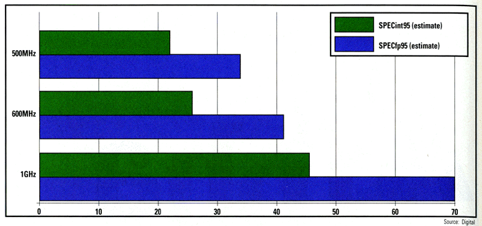 Figure 1: Digital predicts the Alpha 21264 will hit 1 GHz (1000 MHz) in 2000. 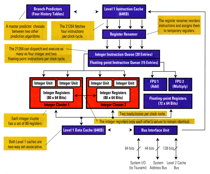 Figure 2: The Alpha 21264 executes up to six instructions per clock cycle. 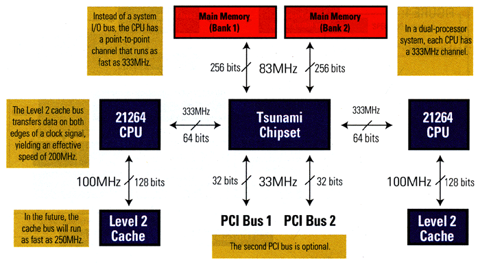 Figure 3: The Tsunami chip set is the key component in 21264-based systems. Letters / August 1999Now you've done it! I've subscribed to the magazine for 3 years, but now I'm really hooked. The articles and columns that Bob Chronister, Mark Russinovich, and Bob Wells write are always satisfying, but Tom R. Halfhill's "The Alpha 21264" (December 1998) captivated me.The article had a message: The Alpha may be the only RISC chip to succeed long term. RISC versus CISC architecture is an important issue to the future of computing, and the Alpha 21264 offers 64-bit processing in an inexpensive package today. I hope we hear more from Tom Halfhill. George Rogers Clark August 6, 1999 |