| Computers evolve in fits and starts. After a period of
five years of relative stasis, Wintel PCs are about to get
their first major improvements since the appearance of the
PCI bus and 66-MHz motherboards in 1992. These changes
will significantly affect buying decisions for anyone
purchasing new systems over the next 18 months. Why is this happening now? Because without an overhaul, the bottlenecks in today's system architectures would greatly cripple the performance of new microprocessors that are soaring to 300MHz and beyond. In addition, new technologies such as digital videodisc (DVD) and the growing use of video and 3-D graphics are overwhelming the ability of main memory and the PCI bus to keep up. The coming changes will also alter the PC industry. They'll probably strengthen Intel's influence, weaken Intel's rivals, reduce the number of component vendors, and replace some open standards with proprietary solutions. Here's what to expect: • CPUI/O buses, now limited to 66 or 75MHz, will accelerate to 83 and 100MHz by early next year. • To match the higher bus frequencies, memory such as fast-page DRAM and extended data out (EDO) DRAM will give way to synchronous DRAM (SDRAM). Starting in 1999, SDRAM will yield to even faster memories, such as SyncLink DRAM (SLDRAM) or Rambus DRAM (RDRAM). • New systems that will be introduced late this year will move the graphics controller off the PCI bus to a private channel called the Accelerated Graphics Port (AGP). This will immediately double or quadruple the graphics throughput. • The 32-bit, 33.3-MHz PCI bus will gradually migrate to a 64-bit bus that will be running at 66.6MHz, especially in high-end PCs. • All new Intel CPUs will address their L2 caches over a private bus to keep traffic off the main I/O bus. Intel will also phase out the industry-standard Socket 7 in favor of its proprietary Slot 1 and Single-Edge Connect (SEC) cartridges. In response, Intel's rivals may resort to in-line caches or an entirely new CPU interface. Driving Faster Buses Modern CPUs usually operate at two clock frequencies. The core (which contains the execution units and the L1 cache) runs at one speed, while the I/O bus (which interfaces the core to memory and peripherals) runs at a slower speed. Users tend to focus on high core speeds without grasping the importance of bus speeds. In the latest microprocessors, the buses lag far behind the cores, seriously impairing the flow of data. CPU bus frequencies have been stuck at 66MHz since Intel introduced the Pentium processor back in 1992. Cyrix's 6x86 and 6x86MX processors can drive their buses at 75MHz, but only a few systems can support that frequency. However, now there's an industrywide push to speeds of 83 and 100MHz. Industrywide is the key word here, because faster buses require much more than faster CPUs. Virtually the entire system has to change — including the core-logic system chip set, the motherboard, and the DRAM. The system chip set consists of two chips that regulate traffic among the CPU, main memory, the L2 cache, the PCI bus, and other peripheral buses — ISA, SCSI, PC Card, universal serial bus (USB), and 1394. Vendors of these chip sets must redesign their components to accommodate these higher frequencies. Some chip sets already support 75 and 83MHz. AMD favors 83MHz as an interim step. "There's no reason why we have to leap directly from 66 to 100MHz," says Vinod Dham, vice president of AMD's computation products group. "We favor a staircase approach that goes from 66 to 83 to 100MHz. This will make it easier for third-party suppliers and still will yield a significant performance advantage." Still, Intel thinks 100MHz is the next logical step. And it commands about 90 percent of the market for CPUs and 80 to 90 percent of the system-chip-set market — and it's the leading motherboard manufacturer, as well. Early next year, Intel plans to release a chip set called the 440BX. It will support bus speeds of 100 MHz with the Pentium II. The 440BX will accompany Intel's introduction of a Pentium II-class processor code-named Deschutes, which will debut at a core frequency of about 350MHz. One reason Intel prefers 100MHz is the impact on the PCI bus. PCI normally runs at a synchronous clock frequency of 33.3 MHz. If the CPU bus rises to 100 MHz, PCI can continue to run synchronously at 33.3 MHz with an even clock multiple of 3X. When the CPU bus runs at 75 MHz, PCI either slows down to 25 MHz (3X) or 30 MHz (2.5X) to maintain a synchronous clock rate or runs asynchronously at 33.3 MHz. All those options hurt performance. Some Cyrix 6x86 systems drive the CPU bus at 75 MHz and the PCI bus at a synchronous 2X frequency of 37.5 MHz, but that's too fast for reliable operation with some PCI cards. If the CPU bus runs at 83 MHz, PCI can run synchronously at a 2.5X multiple of 33.2 MHz. But current Pentium chip sets do not support that multiple. Intel also argues that 100 MHz is inevitable anyway, so the industry might as well take one big step instead of two smaller steps. "From the performance standpoint, we think 100 MHz makes more sense than 83 MHz because it has more headroom," says Jag Bolaria, the marketing director of Intel's platform components division. Intel's jump to 100 MHz will force the industry to go along, but it will also leave some companies behind. There are formidable challenges to making reliable 100-MHz motherboards. They need better power supplies, voltage regulators, and fans to keep the high-wattage CPUs running smoothly. (A 300-MHz Pentium II dissipates 42 W, compared to 17 W for a Pentium-233.) They need shorter traces between critical components to avoid timing delays. Also, they require many improvements to keep internal and external noise from interfering with data signals. To reduce noise, for example, circuit designers must add more capacitors and run their traces in zigzag patterns to avoid long parallel lines that would act as antennas. In the U.S., the 100-MHz bus frequency falls within the FM radio band. A CPU would be confused if it requested some data from memory and instead received a song by Smashing Pumpkins. "It's going to be much harder for the schlocky clone guys to design motherboards at this speed," says Larry Barber, president of Tyan Computer. To squelch noise, Tyan's latest motherboards, and others like them, are sprouting electrolytic capacitors like mushrooms. Jogging Memory Memory has to keep up with faster bus frequencies, as well. Regular DRAMs can't cut it. There is already a migration to SDRAMs, which need wider 168-pin slots on motherboards for dual in-line memory modules (DIMMs) instead of the familiar SIMMs. With today's EDODRAMs on a 66-MHz, 64-bit bus, peak memory bandwidth is 533 MBps. With SDRAMs running at 100 MHz, memory bandwidth will rise to 800 MBps — a healthy boost of 50 percent. Memories will get even faster by 1999. The two most likely successors to SDRAM are SLDRAM and RDRAM. Intel may be the deciding factor here, too, because it has thrown its support behind RDRAM by forging an alliance with Rambus and investing in the company. Rambus does not actually manufacture any RAM; instead, it designs and licenses a proprietary high-speed memory interface to nine leading RAM vendors. Rambus can drive its special 16-bit memory bus at speeds of up to 600 MHz and is adding about 100 MHz per year. By the time RDRAM enters the mainstream, peak bandwidth on a 16-bit bus should be 1.6 GBps — twice as fast as SDRAM at 100 MHz. On a 32-bit bus, bandwidth doubles again to 3.2 GBps. Rambus says its memory bus will eventually run at 1000 MHz (1 GHz), yielding 4GBps of raw bandwidth. SLDRAM is a proposed open standard backed by 22 companies, including Apple, Hewlett-Packard, IBM, Motorola, NEC, and Texas Instruments (but, so far, not Intel). Although the standard isn't final, SLDRAM will be capable of gigabyte transfer rates, too. Ultimately, however, Intel's position as the leading CPU, chip-set, and motherboard supplier will probably determine which one of the memories rules. "If I were betting money, I'd bet on SLDRAM from the technical standpoint and on RDRAM from the political standpoint," says Dean Hays, marketing director at VIA, a chip-set maker. Graphics Detour Another bottleneck in today's PCs is the PCI bus, which Intel introduced in 1992 to relieve the bottleneck that was caused by the ISA bus. PCI isn't keeping up with the growing traffic between the CPU, the graphics controller, and main memory. Users are running higher-resolution screens with more colors, full-motion video, and 3-D graphics, saturating the 133-MBps PCI bus. It doesn't help that the graphics controller must share the bus with other PCI cards. One solution is to widen PCI from its current 32-bit pathway to 64 bits. Another is to double the PCI clock frequency from 33.3 to 66.6 MHz. Each improvement would double the bandwidth, and each is inevitable, but right now they are too costly for most PCs. Doubling the bus width is particularly expensive, because it requires more pins on system chip sets, more traces on motherboards, and more complexity on PCI cards. The 66.6-MHz clock frequency is more economical and will restore some balance to systems with superspeed CPUs. However, Intel is pushing a third alternative: AGP. This solution moves the graphics off the PCI bus altogether and detours the traffic onto a dedicated point-to-point channel between the graphics controller and the system chip set. AGP isn't a bus, because it's not shared by anything but the graphics controller. The controller will have the whole 32-bit channel to itself. The downside is that AGP requires changes to the entire system architecture of Wintel PCs: motherboards, system chip sets, graphics controllers, and graphics cards. Motherboards need a special AGP slot for the new cards, chip sets need a new 32-bit-wide I/O port for the new slot, and graphics controllers and cards need to switch from PCI to AGP protocols. Today's PCs — even the latest multimedia extensions (MMX) systems — aren't upgradable. AGP also needs OS-level support that will not be coming from Microsoft until the next version of Windows (Memphis), which appears to be delayed until 1998. One bright spot is that AGP's protocols are similar to PCI's, somewhat simplifying the design of new chip sets and graphics cards. It's safe to say the hardware will be in place when the software arrives. For instance, Intel will support AGP with its new 440LX chip set, which should debut this fall. Unfortunately, the 440LX works with only Socket 8 (Pentium Pro) and Slot 1 (Pentium II) processors. Intel says it has no plans to support AGP for Socket 7 (Pentium-pin-out) processors — not even the newest MMX Pentiums. Fortunately, other companies (e.g., AMD and VIA) will support AGP on Socket 7 motherboards by releasing new chip sets late this year. Intel's definition of AGP is rather loose, leaving some room for differentiation among chip-set vendors. So-called baseline AGP (or AGP-1x) doubles the graphics bandwidth to 266 MBps (compared to 133 MBps for regular PCI) by doubling the data channel's clock frequency to 66.6 MHz. This minimal implementation will appear in some of the first AGP chip sets and graphics controllers, such as S3's ViRGE/GX2. In 1998, newer graphics controllers and chip sets will implement full AGP (or AGP-2x). This version will quadruple the effective bandwidth to 533 MBps by transferring 32 bits of data on both the rising and falling edges of a 66.6-MHz clock signal, a technique that's known as double pumping. In 1999, AGP-4x will increase the effective bandwidth to more than 1GBps (eight times faster than regular PCI) by cranking up the AGP clock frequency to 133 MHz. Maximizing AGP But there's much more to AGP than faster clocks and double pumping. One option is sideband signaling, which transmits control signals on separate lines instead of on the data channel. This frees up the entire 32-bit channel for graphics — an improvement over PCI, which mixes control signals with data on its 32-bit bus. Not all AGP implementations will have sideband signaling, so this will let vendors differentiate their products. Another AGP option is memory pipelining. This allows the system to handle multiple memory requests from the graphics controller. PCI forces graphics controllers to suspend memory requests if an earlier request is pending — a delay that lengthens the already-long latencies for memory accesses. AGP's pipelining minimizes those delays by queuing the requests. The depth of the queue will be another variable feature in system chip sets; a typical queue might handle possibly a dozen requests. The ability to queue memory requests is particularly important, because AGP graphics controllers can store some data, such as 3-D textures, in main memory instead of in video memory. This might seem illogical, because the specialized memory chips on graphics cards are much faster than ordinary DRAMs. However, some highly detailed 3-D textures are outgrowing video memory, and adding memory to a graphics card is expensive. So AGP lets the graphics controller store the textures in main memory and retrieve them at AGP speeds. When the graphics controller needs to retrieve this data, it sends a request to the system chip set. To save time, the chip set can cache frequently accessed memory addresses in a translation look-aside buffer (TLB), which is similar to the TLBs in microprocessors. If the chip set finds the memory address in the TLB, it quickly jumps to that address and fetches the data — thus requiring only one memory access. If the chip set can't find the requested address in the TLB, it refers to another resource called the graphics address translation table (GATT), also known as the graphics address relocation table (GART). Unlike the TLB, the GART is in main memory, not on the chip set. So it will take one memory access to fetch the address from the GART and another to fetch the data. Obviously, chip sets with larger TLBs are better, because they will hit the cache more often and avoid unnecessary memory fetches. Of course, storing graphics data in main memory means you will have less RAM for programs. But RAM is relatively cheap, and AGP makes the most of it by storing the graphics in small (4KB), noncontiguous blocks allocated at run time. A single graphics object, such as a large 3-D texture, might span several blocks. It remains to be seen how much graphics data AGP controllers actually store in main memory. For one thing, even the specialized memory chips on graphics cards are getting cheaper. Also, graphics controllers are adopting wider and wider I/O interfaces to their dedicated frame buffers. As these interfaces grow from 64 to 128 to 256 ports, the controller chips must grow in size to accommodate the additional pins. They probably won't need all the extra die area for logic, so they could use the leftover space for local memory to cache textures. Still, AGP's ability to store graphics in main memory is a useful option. AGP can also extend the life of the PCI bus. By detouring the graphics onto a dedicated pathway, AGP removes the biggest hog of PCI bandwidth. Intel's Bolaria says the application that demands the most bandwidth is video capturing — it consumes 40 to 50 MBps all by itself. That's more than a third of the bandwidth available on PCI. When AGP shoulders that load, PCI will have more capacity for other things. Slots vs. Sockets Intel's move to a proprietary CPU interface is the final big change coming to Wintel PCs over the next 18 months. The Pentium II and future Intel x86 processors abandon the industry-standard Socket 7 in favor of the Intel-patented Slot 1 and SEC cartridges. (The Pentium Pro fits Socket 8, which is also proprietary to Intel.) Intel's Pentiums and all other x86-compatible processors still use Socket 7, but Intel wants to phase it out as soon as possible. Motherboard manufacturers can license Socket 8 and Slot 1 from Intel; CPU makers cannot. The chances of reverse-engineering those interfaces without provoking legal action from Intel are almost nil, and engineers say it's not practical to put both on the same motherboard. Therefore, motherboard makers must choose between Intel as their sole CPU supplier or Intel's rivals: AMD, Cyrix, and Centaur. It's not much of a choice. With Intel controlling about 90 percent of the CPU market, few companies can afford to bet everything on the competition. Also, Slot 1 and Socket 8 have a technical advantage: They can address an L2 cache over a private bus that runs much faster than the CPU's regular I/O bus. Socket 7 does not have a private cache bus. AMD and Cyrix downplay that difference, but as CPU frequencies escalate, the advantages of a faster L2 cache will become more apparent. One alternative is to compensate by expanding the CPU's L1 cache, but that enlarges the die and the manufacturing cost. Another option is for Intel's rivals to devise their own next-generation CPU interface. Even if they can overcome their own political differences, they will still have to rally support from motherboard and component vendors. A likely stopgap solution is an in-line L2 cache. In this scheme, a daughterboard containing the CPU, L2 cache, and cache controller would plug into Socket 7. External oscillators would overclock the CPU bus for the L2 cache while synchronizing with the motherboard at the usual clock speed. Apple and some Mac-clone vendors are already resorting to this solution to overcome the Mac's slow system bus. The latest Mac clone from Umax runs a PowerPC 603e processor at 300 MHz, an in-line L2 cache at 80 MHz, and the motherboard at 40 MHz. Wintel PCs could do even better, clocking the motherboard at 83 or 100 MHz and the in-line cache at perhaps half the CPU's core frequency. These issues probably won't become critical until 1999. For at least the next year, Socket 7 motherboards will continue to dominate the market, and Socket 7 processors will still offer competitive performance for their target applications. Tidal Wave Major changes come in waves, and Wintel PCs face a tidal wave. Even more innovations are coming, too: NLX motherboards (a 1-millimeter-pitch, 340-pin card-edge device), device-bay expansion slots, and the long-awaited eclipse of ISA, to name just a few. But those changes are mostly for the sake of convenience. The technologies that are outlined here — faster CPU buses, faster memory chips, faster/wider PCI, AGP, and new CPU interfaces — will significantly improve system performance to match the capabilities of superfast microprocessors. They're long overdue, and they'll restore some balance to the overtaxed architectures of today's PCs. Where to Find
AMD
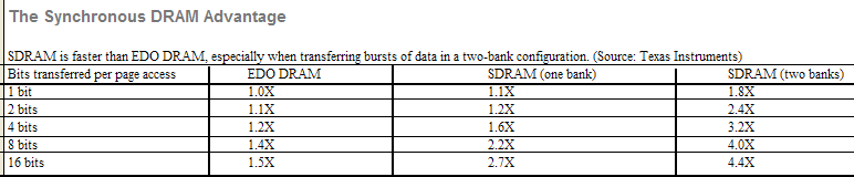
The Synchronous DRAM Advantage
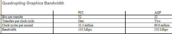
 Quadrupling Graphics Bandwidth
 Five Ways to Faster PCs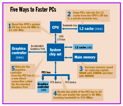 New PCs introduced in coming months will
relieve five internal bottlenecks.
Conventional Graphics Architecture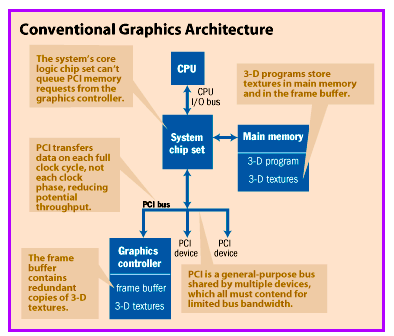 There are several problems with the graphics
architectures of today's PCs.
How Accelerated Graphics Port Works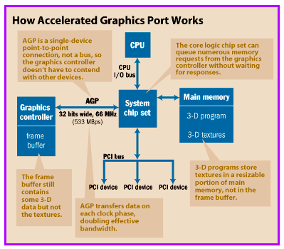 AGP bypasses the PCI bus. Thus, the graphics
controller can access memory four times faster.
Two Buses Are Better Than One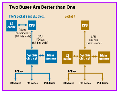 Socket 8 and Slot 1 have two independent
64-bit buses,
improving cache access bandwidth over Socket 7. Tom R. Halfhill is a BYTE senior editor based in San Mateo, California. You can reach him on the Internet at thalfhill@bix.com. Copyright 1994-1998 BYTE |