| DOSSIER: Little is known about the Nx686, because the
chip hasn't been announced yet and NexGen doesn't want to
tip its hand to rivals AMD, Cyrix, and Intel. However,
NexGen has stated that the Nx686 will match the
performance of Intel's P6 and build on the
microarchitecture introduced by the Nx586 in 1994. That microarchitecture, dubbed RISC86 by NexGen, was the first of its kind to appear in an x86 processor. Similar microarchitectures have since been adopted by Intel's P6 and AMD's K5. The basic idea is to convert the troublesome CISC instructions of x86 software into RISC-like operations that execute in parallel within a RISC-like processor core. This approach, known as a decoupled microarchitecture, allows a CISC processor to take advantage of RISC's architectural innovations and be backward-compatibile with existing x86 software. The Nx686 will advance this philosophy to the next logical level. Currently, the Nx586 has three execution units, a three-way superscalar core, and the ability to decode only one x86 instruction per clock. That opens up several opportunities for improvement. The Nx686 will probably have at least five execution units, four execution pipelines, and multiple decoders capable of handling two or more x86 instructions per clock. To cope with the increased complexity of this design, the Nx686 will likely add more rename registers and instruction queues. One thing that won't change is the integrated cache controller and high-speed cache interface. The Nx686, like its predecessor, will talk to its secondary cache over a dedicated I/O bus that runs at the full speed of the processor core. Intel adopted this feature in the P6 and went even further by including a 256-KB static RAM (SRAM) cache in a multichip package. NexGen says it's considering this option because its foundry partner, IBM Microelectronics, is good at making SRAM and multichip modules (MCMs). An example of IBM's MCM technology can be seen in a new version of the Nx586 that's scheduled to ship this quarter and includes both a CPU and an FPU die in an MCM. At the same time, a relayout and a process shrink to 0.35 micron have made it possible for NexGen to dramatically reduce the size of the CPU die to less than 118mm^2 — the smallest in its class. OFFICIAL INTRODUCTION DATE: Unknown (second half of 1996?) CURRENT STATUS: Design stage LIKELIHOOD INTRODUCTION DATE WILL BE MET: Fair TARGET CLOCK SPEED: Unknown ESTIMATED PERFORMANCE: Unknown; probably comparable to that of the Intel P6. FABRICATION PROCESS/FEATURE SIZE: CMOS/0.35- or 0.25-micron TECHNOLOGICAL ADVANTAGES: The Nx686 will enhance the decoupled RISC-like microarchitecture first introduced in the Nx586 while retaining the Nx586's high-speed dedicated cache interface. TECHNOLOGICAL DISADVANTAGES: The Nx686 could reveal the future limits of increased parallelism in a decoupled core. PRIMARY MARKET: Mainstream desktop PCs. Where to Find:NexGen, Inc.A Hint of Things to Come?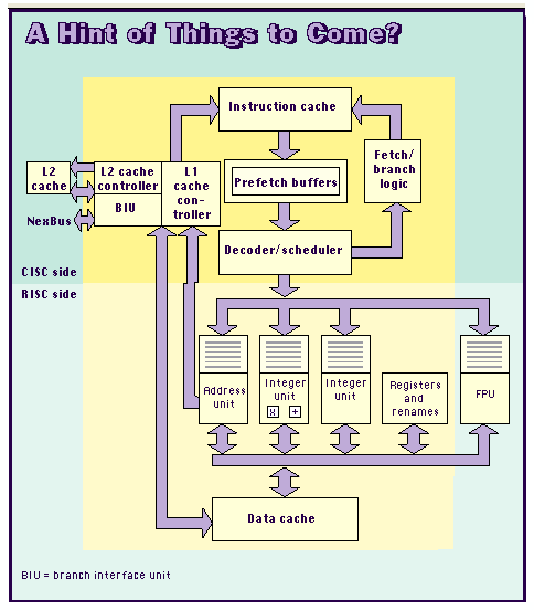 The earlier-generation Nx586 architecture,
shown here, will probably be extended in the Nx686.
Copyright 1994-1998 BYTE |